Creating a Custom Split Keyboard PCB - Part 2
In my last post, I went over my initial design and its issues, which was written after the fact. Here, I’m writing this as I’m actually designing it.
PCB updates
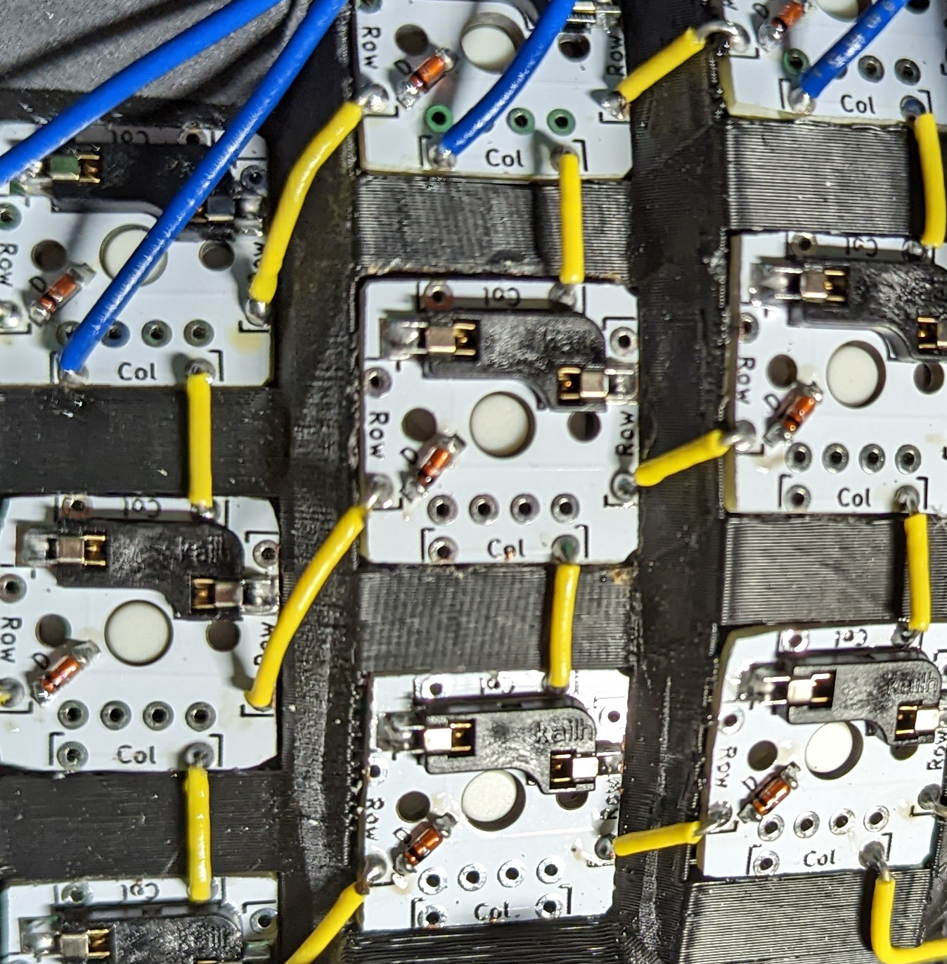
I’ve changed the diode footprint to a MiniMELF footprint. I tried to simply fix the traces, but it got too messy for my liking, and I’ve decided to redo all of the traces. I found that process to be pretty fun, so I’m not bothered by this. I might have had to do this anyway when I moved the thumb buttons. I also removed the reset tac switches.
When I submitted my PCB for fabrication, I was chastised for it actually being two separate boards. I think I might have fixed that. I’ve connected the two boards with mouse bites, so it should count as a single board. I’ve also changed the position of the switch references on the silkscreen so they’re better hidden. I’ve made some other minor changes as well, like tweaks to the spacing between keys, and a cleaner edge cuts design.

Next, I’ll do the traces.
Traces
Maybe it’s because of the novelty of the process, but this is sort of fun at this point. Well, backing up a moment, first, ground planes must be put in place. Simply put, a ground plane is covering a layer of the board almost entirely with copper connected to ground. This has a lot of benefits, including reducing EMI and making routing easier. Filling these in is pretty easy, I just trace around to board’s edge cuts to define zones, then fill them in.

I also took this opportunity to flip the MCUs. The supplier sent me two Elite-Cs of different versions, so the ATmega chip had a different footprint. Let’s hide that little inconsistency. With that out of the way, it’s time to trace leads. I started by connecting VCC and transmit pins. There’s no need to run traces to any GND pins, since they will be in contact with the ground plane I set up in the last step.

I remember from last time, the tricky part was this step. The key here, AFAIK, is to try to make it so the ground planes are one solid piece on each side. So that involves making sure there’s enough space for the plane to “flow” through. There is a decent margin that must be left for this, so it’s harder than it might seem. Not very hard, but not mindless. My plan is to start on the outside, or top, and work my way in, or down. I figure that will require the least amount of creative routing.
Otherwise, the only other thing that I’m aware of, in my limited, hobbyist understanding, is that you should avoid 90 degree or more bends. I guess it can cause issues with the electricity bouncing around those corners? My understanding of how electricity works is basic best. As long as I periodically check the 3D render to make sure I haven’t broken the ground plane, I should be all set.
I thought there might be some sort of limit or “code smell” of sorts for having lots of vias, but apparently the only real limit is how much the fabricator is willing to put on there. This is good news for me, because I’d like there to be as few visible traces on the front of the board as possible. For, you know, aesthetics.
Trace routing challenges
I’m running into some issues getting all the traces neatly routed, so I did a bit more research, and found that I can indeed use 90 degree turns. Apparently this sort of thing only matters for high speed, whatever that means. Everything I found indicated that a keyboard is nowhere near high speed. Having an uninterrupted ground plane probably doesn’t matter much for this application, either.
I’ve just finished running all of the traces. I’m happy with how they turned out. The second side was easier of course, since the lessons of the first side were fresh in my head from routing them this morning. The main lesson is: if you’re working your way from the outside in, make sure that you haven’t forgotten any traces. Turning the rats nest on really helps for this.


Production
Now, it’s just a matter of preparing the gerber file and submitting it for production! In KiCad, you make a gerber file by going File > Plot. In that menu, you click generate, as well as creating the drill and map files. The exact settings needed here will depend on what format your fabricator requires. Then you can just zip up all those files, and you have your gerber file. Of course, I have made all of these available on my GitHub.
I’ve submitted the file to my fabricator, and now we wait. In the next part, I’ll go through the process of assembly.
EDIT: Of course, shortly after submitting them, I realized that since I’ve fixed the orientation of the MCUs, the on-board reset button will no longer be accessible. Oh well, I can always reset it with a key combination. Perhaps if there’s a revision to this I will add it back in.
